In the study of transistors it was pointed out that the solid state diode is
manufactured from semiconductor material. It consists of N-type and P-type
material joined in a single crystal. The point, or junction, where the two
materials are in contact is called a P-N junction. This type of semiconductor,
regardless of rating or size, is called a junction diode. The first type of
semiconductor used was called the point contact diode. It utilized a single type
of semiconductor material, against which a tungsten or phosphor-bronze wire,
called a "cat whisker," was pressed or fused. The point contact diode has been
largely replaced by the junction diode because of its limited current carrying
capabilities. The most common semiconductor materials are germanium and silicon.
A typical junction diode is shown in
figure 8-235.
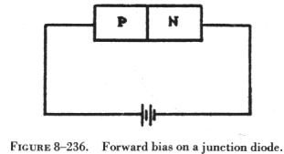
| In figure 8-236, the positive terminal of the battery is connected to the P-type semiconductor material, and the negative terminal is connected to the N-type. This arrangement constitutes forward bias. The holes in the P-type material are repelled from the positive terminal and move toward the junction. The electrons in the N-type material are repelled from the negative terminal and likewise move toward the junction. This decreases the space charge existing at the junction, and electron current flow is maintained through the external circuit. The current in the P-type material is in the form of holes, and in the N-type material it is in the form of electrons. If the forward bias is increased, current flow will increase. If the forward bias is increased excessively, it will cause excessive current. The excessive current will increase thermal agitation and the crystal structure will break down. One important fact worth remembering is that all solid state devices are sensitive to heat and will be destroyed if the heat becomes too intense. |
|
If the battery connections shown in figure 8-236 are reversed, the junction
diode is reverse biased. Now the holes are attracted toward the negative
terminal and away from the junction. The electrons are attracted toward the
positive terminal, also away from the junction. This widens the depletion
region, increases the space charge, and reduces current to a minimum condition.
It is possible to apply too high a reverse bias. When this happens, the crystal
structure will break down, and the diode is fried!
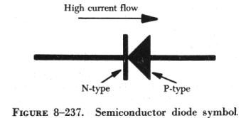 |
The symbol for the semiconductor diode is shown in figure 8-237. Note
that this is the same symbol used for other types of diodes, such as the
copper oxide and selenium dry disk rectifiers. The forward bias, or high
current, direction is always against the arrow of the symbol.
Figure 8-238 shows a typical characteristic curve for a junction diode. As forward bias is increased a small amount, current flow is increased a considerable amount. For this reason, solid state devices are said to be current operated devices, since it is easier to measure the relatively large changes in current flow as compared to the small changes in applied voltage. With forward bias applied, the diode displays a low resistance characteristic. On the other hand, with reverse bias applied, a high resistance state exists. The most important characteristic of a diode is that it allows current to flow in one direction only. This permits solid state devices to be used in rectifier circuits. |